


In the mid-2020s, the high-performance computing (HPC) and artificial intelligence industries faced a fundamental physics problem. Moore’s Law, which predicted a doubling of transistor counts, continued to hold true, but an imbalance emerged: GPU compute cores became so fast that the memory subsystem could no longer keep up with the data. This phenomenon became known as the ” Memory Wall.”
While capacity was the bottleneck in the HBM2e and HBM3 era, by the time architectures like NVIDIA Rubin and AMD Instinct MI400 were announced, bandwidth and energy efficiency of bit-transferring information had become critical. The industry’s response was the HBM4 (High Bandwidth Memory Generation 4) standard —a technology that changes not just speed but the very paradigm of chip design.
Below is a detailed analysis of the architecture, manufacturing challenges, and market prospects of HBM4.
Part 1. Architectural Revolution: Why Change the Rules of the Game?
The transition from HBM3e to HBM4 is not an evolutionary frequency increase, as is the case with the GDDR standard. It is a radical change in the interface architecture, enshrined in JEDEC standards (JESD270-4).
1.1. Bus expansion: From 1024 to 2048 bits
Up to and including the HBM3e generation, each DRAM stack communicated with the processor (Host GPU/ASIC) via a 1024-bit interface. To increase throughput, engineers had to constantly increase the memory clock frequency. However, the physics of memory wiring is unforgiving: increasing the frequency leads to a nonlinear increase in heat dissipation and signal integrity issues.
In HBM4, the industry went “wider”:
- Interface width: Doubled to 2048 bits per stack.
- The point of the change: Doubling the number of data transfer channels allows for a reduction in the memory clock frequency while simultaneously increasing the overall throughput.
- Result: The peak throughput of a single stack exceeded 1.5–1.65 TB/s (terabytes per second). For comparison, a standard DDR5 module in a consumer PC delivers around 60–70 GB/s. A single HBM4 stack is more than 20 times faster, and there can be 8 or 12 such stacks on a single GPU.
1.2. 16-Hi Stack
The HBM4 standard was originally designed for vertical integration of 16 layers of DRAM dies (16-Hi). In previous generations, 8-Hi and 12-Hi were the standard. The move to 16 layers allows for a dramatic increase in memory density. A single HBM4 stack can have a capacity of 48 GB or even 64 GB . This is critical for LLM (Large Language Models), where the model parameters (weights) must fit entirely within VRAM for efficient inference.
Part 2. The Basic Crystal: Memory Goes Smart
The most significant change in HBM4, often overlooked in cursory reviews, is the transformation of the Base Die .
2.1. Rejection of memory process technologies
In HBM3e, the base die, which serves as the foundation for the stack and the signal switch, was manufactured using the same process technology as the DRAM itself. This is inexpensive, but places limitations on the logic.
In HBM4, the base crystal is manufactured at third-party foundries such as TSMC using the following logical process technologies :
- 12nm FFC+ (FinFET Compact): For cost-effective solutions.
- 5nm (N5): For high-performance solutions.
2.2 Why do we need logic in memory?
The use of a 5-nanometer process technology for the base layer opens the era of Processing-In-Memory (PIM) or Near-Memory Computing.
- Intelligent Routing: More sophisticated controllers inside the memory can optimize data flows.
- RAS (Reliability, Availability, Serviceability): Built-in error correction mechanisms (ECC) become much more powerful, which is necessary at enormous bit densities.
- Reduced power consumption: The logic process technology allows for a lower interface supply voltage, which compensates for the increase in the number of channels.
This turns HBM4 into not just a “storage” unit, but an active coprocessor that takes over routine operations, offloading the main data bus.
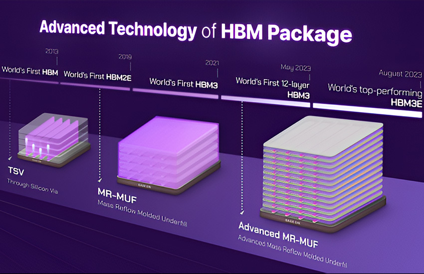
Part 3. Manufacturing War: Hybrid Bonding vs. MR-MUF
Packaging technologies are where the main intrigue and misconceptions lie. The original article claimed that the industry had completely abandoned micro-bumps in favor of hybrid bonding. This isn’t entirely true, and the reality is far more complex and interesting.
3.1 The problem of altitude and heat
A 16-layer silicon stack is physically taller than an 8- or 12-layer stack. However, JEDEC specifications strictly limit the overall module height (720 microns) to fit under standard heatsinks and into the 2.5D packaging architecture (CoWoS).
- The challenge: Make the silicon layers themselves thinner and reduce the gaps between them.
- Risk: Wafer thinning causes brittleness and warpage when heated.
3.2. SK Hynix Strategy: Evolution of MR-MUF
SK Hynix , which holds over 50% of the HBM market and is a major supplier to NVIDIA, hasn’t abandoned bumpers in HBM4. They use an improved Advanced MR-MUF (Mass Reflow Molded Underfill) technology .
- The essence of the method: The layers are connected with micro-bumps (tin-lead balls), and the space between them is filled with a special liquid compound (Mold), which then hardens.
- Advantage: MR-MUF provides better heat dissipation (the compound acts as a heat conductor) and reduces pressure on fragile crystals during installation.
- HBM4 implementation: SK Hynix managed to reduce the bump size and the pitch enough to fit 16 layers into a standard height, while maintaining reliability and a high yield.
3.3. Samsung Strategy: Bet on Hybrid Bonding
Samsung Electronics, trying to catch up with its competitor, is investing more actively in Hybrid Bonding (HCB – Hybrid Copper Bonding) .
- The method involves direct copper-to-copper bonding without the use of solder (bumps). The silicon layers are polished to a perfect mirror finish and bonded using van der Waals forces and subsequent annealing.
- Advantage: Allows to achieve the minimum possible stack thickness and better electrical conductivity.
- Disadvantages: Extreme manufacturing complexity. Even the smallest speck of dust, measuring just a few nanometers, between layers can result in the entire stack being defective. This makes the technology very expensive and, at present, not widely used.
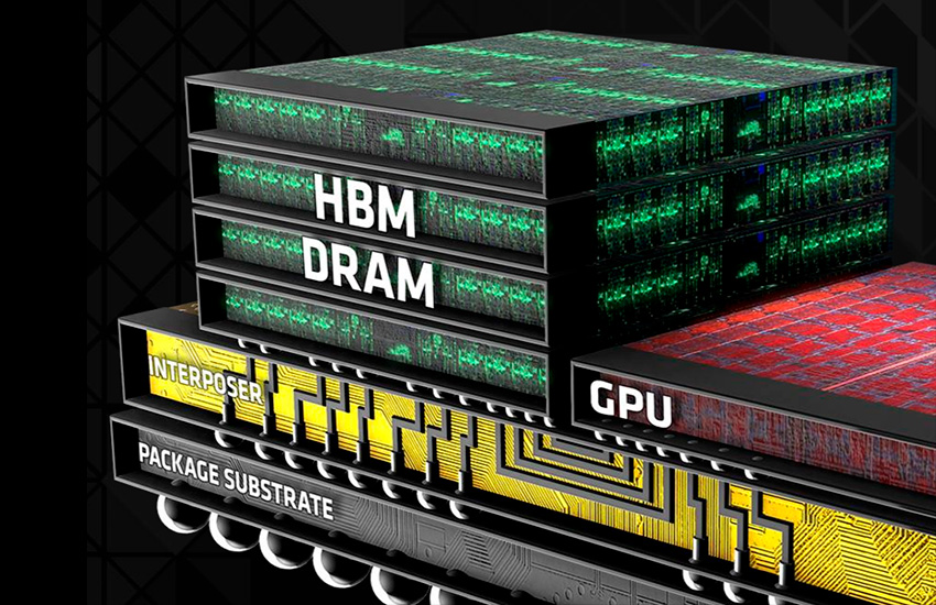
Part 4. Integration and Ecosystem: CoWoS and Interposers
HBM4 memory itself is useless without a processor. They are combined on the substrate using CoWoS (Chip-on-Wafer-on-Substrate) technology, promoted by TSMC.
4.1. Interposer problem
HBM4, with its 2048-bit bus, requires twice as many contact pads on the interposer (the silicon substrate that connects the memory and the GPU).
- Standard interposers (Reticle limit) have already reached their size limit.
- HBM4 and new GPUs use CoWoS-L (Local Silicon Interconnect) and CoWoS-R technologies . These technologies allow multiple interposers to be stitched together, creating gigantic chips three to four times larger than the photomask size.
4.2. TSMC’s Role
Taiwanese giant TSMC is becoming more than just a chip manufacturer, but a systems integrator. Their ability to seamlessly integrate a GPU (manufactured on a 3nm process) and HBM4 Base Die (manufactured on a 5nm process) into a single package is key to the success of NVIDIA and AMD.
Part 5. Energy Efficiency and Physics
Why is HBM4 so important for data center ecology?
5.1. pJ/bit metric
The main efficiency metric is the number of picojoules of energy expended to transfer one bit of data. In GDDR6X, this figure is high due to the long traces on the PCB. In HBM4, thanks to microscopic distances (via TSVs – Through-Silicon Vias) and a wide bus, this figure is reduced to record lows.
5.2 Thermal throttling
Despite its efficiency, the 16-layer packaging density creates colossal thermal density. While HBM3e reached temperatures of 85-90°C, HBM4 requires even more sophisticated cooling systems. This is driving the transition of servers to Direct Liquid Cooling, as air alone is no longer sufficient to dissipate heat from assemblies consuming 1000-1200W (GPU + HBM).
Part 6. Market Realities and Timing (Fact-Checking)
Based on data as of the end of 2025, the market situation looks as follows:
- Sampling: SK Hynix and Samsung have indeed begun shipping 12-Hi and 16-Hi HBM4 engineering samples to key partners (NVIDIA, AMD, Google) in the second half of 2025. This is necessary for qualifying and debugging memory controllers in new GPUs.
- Volume Production: Full production line launch for commercial sales is planned for the first half of 2026.
- First Products: The first devices to feature HBM4 are expected to be NVIDIA Rubin (R100) series accelerators and updated AMD Instinct MI450 series , both of which are expected to be announced in 2026.
The claim that HBM4 will already be commercially available in 2025 is an exaggeration. In 2025, HBM3e (in the H200 and Blackwell B200 accelerators) will rule the roost.
Part 7. HBM4 vs. GDDR7: Why Not for Gamers?
A common user question: “When will HBM4 appear on my GeForce RTX 6090?” The answer: never . Here’s why:
- Cost: A single HBM3e/4 stack costs tens of times more than a GDDR7 chip of the same capacity. The complexity of CoWoS packaging makes the production of graphics cards with HBM economically unfeasible for the consumer market.
- GDDR7: The new GDDR7 graphics memory standard has also hit the market. It offers speeds of up to 32-40 Gbps per pin and uses PAM3 encoding. For gaming applications that don’t require simultaneous access to 192 GB of memory with 6 TB/s of bandwidth, GDDR7 offers the ideal balance of price and performance.
HBM4 will remain the prerogative of the Enterprise segment, supercomputers and AI clusters.